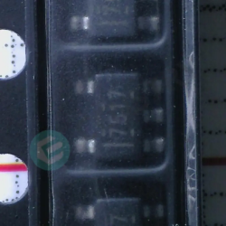
IC GATE DRVR LOW-SIDE SOT23-5


Las imágenes son sólo para referencia..
Consulte las Especificaciones del producto para obtener detalles del producto.
IC GATE DRVR LOW-SIDE SOT23-5
Los pedidos superiores a $200 son elegibles para un regalo de estilo chino de edición limitada.
Los pedidos superiores a $1000 califican para una exención de tarifa de envío de $30.
Los pedidos que superen los $5000 disfrutan de la exención de tarifas de envío y transacción.
Estas ofertas son aplicables tanto a clientes nuevos como existentes y son válidas desde el 1 de enero de 2024 hasta el 31 de diciembre de 2024..
TI
UCC27517DBVR datasheet
SOT23-5
Chips IC
 Lead free/RoHS Compliant
Envíe su solicitud de cotización ahora y esperamos brindarle una cotización dentro de mayo 06, 2024. Realice su pedido ahora y esperamos completar la transacción dentro de mayo 08, 2024. Ps: La hora es según GMT+8:00.


1 FEATURES
• Low-Cost, Gate-Driver Device Offering Superior Replacement of NPN and PNP Discrete Solutions
• 4-A Peak Source and 4-A Peak Sink Symmetrical Drive
• Fast Propagation Delays (13-ns typical)
• Fast Rise and Fall Times (9-ns and 7-ns typical)
• 4.5-V to 18-V Single Supply Range
• Outputs Held Low During VDD UVLO (ensures glitch free operation at power-up and power-down)
• TTL and CMOS Compatible Input Logic Threshold (independent of supply voltage)
• Hysteretic Logic Thresholds for High Noise Immunity
• Dual Input Design (choice of an inverting (IN-pin) or non-inverting (IN+ pin) driver configuration)
– Unused Input Pin can be Used for Enable or Disable Function
• Output Held Low when Input Pins are Floating
• Input Pin Absolute Maximum Voltage Levels Not Restricted by VDD Pin Bias Supply Voltage
• Operating Temperature Range of -40°C to 140°C
• 5-Pin DBV (SOT-23) and 6-Pin DRS (3 mm x 3 mm WSON with exposed thermal pad) Package Options
2 APPLICATIONS
• Switch-Mode Power Supplies
• DC-to-DC Converters
• Companion Gate Driver Devices for Digital Power Controllers
• Solar Power, Motor Control, UPS
• Gate Driver for Emerging Wide Band-Gap Power Devices (such as GaN)
3 DESCRIPTION
The UCC27516 and UCC27517 single-channel, high-speed, low-side gate driver devices are capable of effectively driving MOSFET and IGBT power switches. Using a design that inherently minimizes shoot-through current, UCC27516 and UCC27517 are capable of sourcing and sinking high, peak-current pulses into capacitive loads offering rail-to-rail drive capability and extremely small propagation delay typically 13 ns.
The UCC27516 and UCC27517 provides 4-A source, 4-A sink (symmetrical drive) peak-drive current capability at VDD = 12 V.
The UCC27516 and UCC27517 is designed to operate over a wide VDD range of 4.5 V to 18 V and wide temperature range of -40°C to 140°C. Internal Under Voltage Lockout (UVLO) circuitry on VDD pin holds output low outside VDD operating range. The capability to operate at low voltage levels such as below 5 V, along with best in class switching characteristics, is especially suited for driving emerging wide band-gap power switching devices such as GaN power semiconductor devices.
UCC27516 and UCC27517 features a dual-input design which offers flexibility of implementing both inverting (IN-pin) and non-inverting (IN+ pin) configuration with the same device. Either IN+ or IN- pin can be used to control the state of the driver output. The unused input pin can be used for enable and disable function. For safety purpose, internal pull-up and pull-down resistors on the input pins ensure that outputs are held low when input pins are in floating condition. Hence the unused input pin cannot be left floating and needs to be properly biased to ensure that driver output is in enabled for normal operation.
The input pin threshold of the UCC27516 and UCC27517 devices are based on TTL and CMOS-compatible low- voltage logic which is fixed and independent of the VDD supply voltage. Wide hysteresis between the high and low thresholds offers excellent noise immunity.


Request a quote UCC27517DBVR at censtry.com. All items are new and original with 365 days warranty! The excellent quality
and guaranteed services of UCC27517DBVR in stock for sale, check stock quantity and pricing,
view product specifications, and order contact us:sales@censtry.com.
The price and lead time for UCC27517DBVR depending on the quantity required, please send your request to us,
our sales team will provide you price and delivery within 24 hours, we sincerely look forward to cooperating with you.

TI
6211 PCS
TMS29F04090C5DDE .PDF
TI
20 PCS
AN74ALS245AN .PDF
TI
294 PCS
AM26S10CN .PDF
TI
529 PCS
AM26S10CDR .PDF
2024-05-05
Just did a large order with Censtry in China and they were excellent.
2024-05-04
I will give a 5 star.
2024-05-04
Good company to do business .
2024-05-03
Great company. Excellent prices and quality parts.
2024-05-02
Good supplier!!
2024-04-28
Good parts, excellent service, quick shipment. Thanks Katie and Nichole
2024-04-22
I recommend! Fast delivery and high quality product!
2024-04-08
Received the product without any problem. Fast shipping and reasonable prices. I recommend this store.
2024-03-13
Great company to work with, always quotes great and delivers on time...Dean is great!!!
2024-01-19
great company, we wish a great cooperation in the future!

Valoramos mucho sus comentarios. Comparta su reseña más genuina.
*Por favor, inicie sesión en su cuenta antes de publicar un comentario