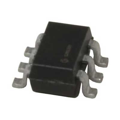
IC PWR SWITCH N-CHAN 1:1 SOT23-6


Las imágenes son sólo para referencia..
Consulte las Especificaciones del producto para obtener detalles del producto.
IC PWR SWITCH N-CHAN 1:1 SOT23-6
Los pedidos superiores a $200 son elegibles para un regalo de estilo chino de edición limitada.
Los pedidos superiores a $1000 califican para una exención de tarifa de envío de $30.
Los pedidos que superen los $5000 disfrutan de la exención de tarifas de envío y transacción.
Estas ofertas son aplicables tanto a clientes nuevos como existentes y son válidas desde el 1 de enero de 2024 hasta el 31 de diciembre de 2024..
TI
TPS22918TDBVTQ1 datasheet
SOT-23-6
Chips IC
 Lead free/RoHS Compliant
Envíe su solicitud de cotización ahora y esperamos brindarle una cotización dentro de abril 30, 2024. Realice su pedido ahora y esperamos completar la transacción dentro de mayo 02, 2024. Ps: La hora es según GMT+8:00.


1 Features
• AEC-Q100 Qualified
• Integrated single-channel load switch
• Qualified for automotive applications:
– Device Temperature Grade 2: –40°C to
+105°C ambient operating temperature range
• Functional safety capable
– Documentation available to aid functional safety system design
• Input voltage range: 1 V to 5.5 V
• Low On-Resistance (RON)
– RON = 52 mΩ (typical) at VIN = 5 V
– RON = 53 mΩ (typical) at VIN = 3.3 V
• 2-A Maximum continuous switch current
• Low quiescent current
– 8.3 µA (typical) at VIN = 3.3 V
• Low-control input-threshold enables use of 1 V or higher GPIO
• Configurable Quick-Output Discharge (QOD)
• Configurable rise time with CT pin
• Small SOT23-6 package (DBV)
– 2.9 mm × 2.8 mm, 0.95-mm Pitch,
1.45-mm height (with leads)
• ESD Performance tested per AEC Q100
– ±2-kV HBM and ±750-V CDM
2 Applications
• Automotive electronics
• Infotainment
• Cluster
• ADAS (Advanced Driver Assistance Systems)
3 Description
The TPS22918-Q1 is a single-channel load switch with both configurable rise time and configurable quick-output discharge. The device contains an Nchannel MOSFET that can operate over an input voltage range of 1 V to 5.5 V and can support a maximum continuous current of
2 A. The switch is controlled by an on and off input, which is capable of interfacing directly with lowvoltage control signals.
The configurable rise time of the device reduces inrush current caused by large bulk load capacitances, thereby reducing or eliminating power supply droop. The TPS22918-Q1 features a configurable quick output discharge (QOD) pin, which controls the fall time of the device to allow design flexibility for power down and sequencing.
The TPS22918-Q1 is available in a small, leaded SOT-23 package (DBV) which allows to visually inspect solder joints. The device is characterized for operation over the free-air temperature range of –40°C to +105°C.

Request a quote TPS22918TDBVTQ1 at censtry.com. All items are new and original with 365 days warranty! The excellent quality
and guaranteed services of TPS22918TDBVTQ1 in stock for sale, check stock quantity and pricing,
view product specifications, and order contact us:sales@censtry.com.
The price and lead time for TPS22918TDBVTQ1 depending on the quantity required, please send your request to us,
our sales team will provide you price and delivery within 24 hours, we sincerely look forward to cooperating with you.
TI
6211 PCS
TMS29F04090C5DDE .PDF
TI
20 PCS
AN74ALS245AN .PDF
TI
294 PCS
AM26S10CN .PDF
TI
529 PCS
AM26S10CDR .PDF
2024-04-29
Worked fine thanks
2024-04-28
Very good parts company.
2024-04-28
tutto ok grazie
2024-04-28
Excellent packaging, good price
2024-04-27
excelent part and funtionally is great working at 100%
2024-04-26
composant conforme a l'annonce ,mer?i .

Valoramos mucho sus comentarios. Comparta su reseña más genuina.
*Por favor, inicie sesión en su cuenta antes de publicar un comentario