WSON-6 21+


Las imágenes son sólo para referencia..
Consulte las Especificaciones del producto para obtener detalles del producto.
WSON-6 21+
Los pedidos superiores a $200 son elegibles para un regalo de estilo chino de edición limitada.
Los pedidos superiores a $1000 califican para una exención de tarifa de envío de $30.
Los pedidos que superen los $5000 disfrutan de la exención de tarifas de envío y transacción.
Estas ofertas son aplicables tanto a clientes nuevos como existentes y son válidas desde el 1 de enero de 2024 hasta el 31 de diciembre de 2024..
TI
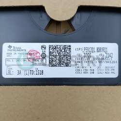
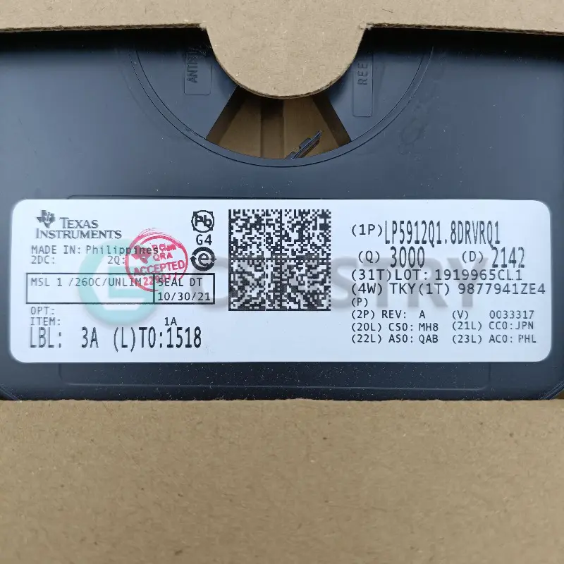
LP5912Q1.8DRVRQ1 datasheet
WSON-6
Circuitos integrados de RF
 Lead free/RoHS Compliant
Envíe su solicitud de cotización ahora y esperamos brindarle una cotización dentro de junio 03, 2024. Realice su pedido ahora y esperamos completar la transacción dentro de junio 06, 2024. Ps: La hora es según GMT+8:00.


1 Features
• Qualified for Automotive Applications
• AEC Q100-Qualified With the Following Results
– Device Temperature Grade 1: –40°C to +125°C Ambient Operating Temperature Range
– Device HBM Classification Level 2 – Device CDM Classification Level C6
• Input Voltage Range: 1.6 V to 6.5 V
• Output Voltage Range: 0.8 V to 5.5 V • Output Current up to 500 mA
• Low Output Voltage Noise: 12 µVRMS Typical
• PSRR at 1 kHz: 75 dB Typical
• Output Voltage Tolerance (VOUT ≥ 3.3 V): ±2%
• Low IQ (Enabled, No Load): 30 µA Typical
• Low Dropout (VOUT ≥ 3.3 V): 95 mV Typical at 500-mA Load
• Stable With 1-µF Ceramic Input and Output Capacitors
• Thermal-Overload and Short-Circuit Protection
• Reverse Current Protection
• No Noise Bypass Capacitor Required
• Output Automatic Discharge for Fast Turnoff
• Power-Good Output With 140-µs Typical Delay
• Internal Soft-Start to Limit the In-rush Current
• –40°C to +125°C Operating Junction Temperature Range
2 Applications
• Camera Modules
• Sensors
• HiFi Audio Radio Transceivers
• PLL/Synthesizer, Clocking
• Medium-Current, Noise-Sensitive Applications
3 Description
The LP5912-Q1 is an LDO capable of supplying 500-mA output current. Designed to meet the requirements of RF and analog circuits, the LP5912-Q1 device provides low noise, high PSRR, low quiescent current, and low line and load transient response. The LP5912-Q1 offers class-leading noise performance without a noise bypass capacitor and with the ability for remote output capacitance placement.
The device is designed to work with a 1-µF input and a 1-µF output ceramic capacitor (no separate noise bypass capacitor required).
This device is available with fixed output voltages from 0.8 V to 5.5 V in 25-mV steps. Contact Texas Instruments Sales for specific voltage option needs.


Request a quote LP5912Q1.8DRVRQ1 at censtry.com. All items are new and original with 365 days warranty! The excellent quality
and guaranteed services of LP5912Q1.8DRVRQ1 in stock for sale, check stock quantity and pricing,
view product specifications, and order contact us:sales@censtry.com.
The price and lead time for LP5912Q1.8DRVRQ1 depending on the quantity required, please send your request to us,
our sales team will provide you price and delivery within 24 hours, we sincerely look forward to cooperating with you.
TI
8000 PCS
LMD18201T .PDF
TI
4470 PCS
INA240A3PWR .PDF
TI
62900 PCS
TPS7B8250QDRVRQ1 .PDF
TI
380948 PCS
TPS7B8150QDRVRQ1 .PDF
2024-06-02
Как обычно, всё отлично. Спасибо!
2024-06-02
very neatly wrapped components, recommended seller.
2024-06-01
Todo muy bien, gracias
2024-05-31
Artigo de qualidade bom pre?o entrega rapido embalagem na perfei?ao recomenda-se que compre neste vendedor.
2024-05-28
Prodotto ok. FEDEX mai più. Spese doganali il doppio del valore della merce
2024-05-23
welson is easy to work with.... and efficient and friendly.
2024-05-12
We goofed and double paid an invoice to Censtry. They caught the error and called us! Thank you Censtry elec for your INTEGRITY!
2024-04-21
very reliable
2024-03-09
Very good customer Service


Valoramos mucho sus comentarios. Comparta su reseña más genuina.
*Por favor, inicie sesión en su cuenta antes de publicar un comentario