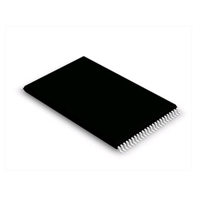
Buffer 2-CH Non-Inverting CMOS 6-Pin TSOP T/R


Las imágenes son sólo para referencia..
Consulte las Especificaciones del producto para obtener detalles del producto.
Buffer 2-CH Non-Inverting CMOS 6-Pin TSOP T/R
Los pedidos superiores a $200 son elegibles para un regalo de estilo chino de edición limitada.
Los pedidos superiores a $1000 califican para una exención de tarifa de envío de $30.
Los pedidos que superen los $5000 disfrutan de la exención de tarifas de envío y transacción.
Estas ofertas son aplicables tanto a clientes nuevos como existentes y son válidas desde el 1 de enero de 2024 hasta el 31 de diciembre de 2024..
NXP
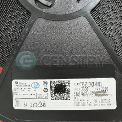
74LVC2G34GV.125 datasheet
TSOP
Chips IC
 Lead free/RoHS Compliant
Envíe su solicitud de cotización ahora y esperamos brindarle una cotización dentro de mayo 03, 2024. Realice su pedido ahora y esperamos completar la transacción dentro de mayo 08, 2024. Ps: La hora es según GMT+8:00.


FEATURES
• Wide supply voltage range from 1.65 V to 5.5 V
• 5 V tolerant input/output for interfacing with 5 V logic
• High noise immunity
• Complies with JEDEC standard:
– JESD8-7 (1.65 V to 1.95 V)
– JESD8-5 (2.3 V to 2.7 V)
– JESD8B/JESD36 (2.7 V to 3.6 V).
• ESD protection:
– HBM EIA/JESD22-A114-B exceeds 2000 V
– MM EIA/JESD22-A115-A exceeds 200 V.
• ±24 mA output drive (VCC = 3.0 V)
• CMOS low power consumption
• Latch-up performance exceeds 250 mA
• Direct interface with TTL levels
• Multiple package options
• Specified from −40 °C to +85 °C and
−40 °C to +125 °C.
DESCRIPTION
The 74LVC2G34 is a high-performance, low-power,
low-voltage, Si-gate CMOS device and superior to most
advanced CMOS compatible TTL families.
Inputs can be driven from either 3.3 V or 5 V devices.
These feature allows the use of these devices as
translators in a mixed 3.3 V and 5 V environment.
This device is fully specified for partial power-down
applications using Ioff. The Ioff circuitry disables the output,
preventing the damaging backflow current through the
device when it is powered down.
The 74LVC2G34 provides two buffers.


Request a quote 74LVC2G34GV.125 at censtry.com. All items are new and original with 365 days warranty! The excellent quality
and guaranteed services of 74LVC2G34GV.125 in stock for sale, check stock quantity and pricing,
view product specifications, and order contact us:sales@censtry.com.
The price and lead time for 74LVC2G34GV.125 depending on the quantity required, please send your request to us,
our sales team will provide you price and delivery within 24 hours, we sincerely look forward to cooperating with you.
SAMSUNG
1 PCS
KHA884901X-MC13 .PDF
INTEL
1351 PCS
5M160ZE64C4N .PDF
XILINX
611 PCS
XC3S200-4FT256I .PDF
TI
1343 PCS
TPS65100QPWPRQ1 .PDF
2024-05-02
I hope we can do more buisness in the Future.
2024-05-02
It was a pleasure to work with Susan at Censtry. Thank you
2024-05-01
John Walsh is great to work and is very professional.
2024-05-01
Kevin fast shipper ,RECOMMENDED !
2024-04-29
Lizzeth was a joy to work with.
2024-04-27
Melissa in Censtry Electronics is the best !
2024-04-21
My transaction with Andy was great. He is a nice man and working with him was super easy and fast.
2024-04-11
NICE TO WORK WITH CENSTRY
2024-03-20
Original parts received, good supplier
2024-02-07
Censtry elec, A Great Company
Valoramos mucho sus comentarios. Comparta su reseña más genuina.
*Por favor, inicie sesión en su cuenta antes de publicar un comentario