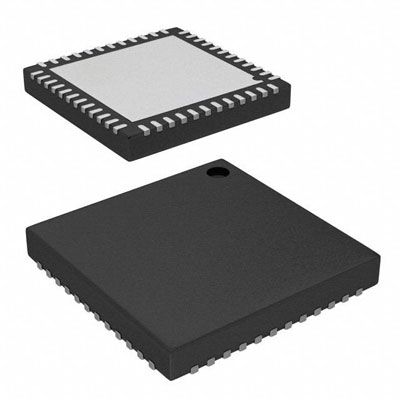
POWER MANAGEMENT UNIT, 5 O/P, VQFN-48


Las imágenes son sólo para referencia..
Consulte las Especificaciones del producto para obtener detalles del producto.
POWER MANAGEMENT UNIT, 5 O/P, VQFN-48
Los pedidos superiores a $200 son elegibles para un regalo de estilo chino de edición limitada.
Los pedidos superiores a $1000 califican para una exención de tarifa de envío de $30.
Los pedidos que superen los $5000 disfrutan de la exención de tarifas de envío y transacción.
Estas ofertas son aplicables tanto a clientes nuevos como existentes y son válidas desde el 1 de enero de 2024 hasta el 31 de diciembre de 2024..
TI
TPS65217CRSL datasheet
VQFN-48
Circuitos integrados de RF
 Lead free/RoHS Compliant
Envíe su solicitud de cotización ahora y esperamos brindarle una cotización dentro de abril 21, 2024. Realice su pedido ahora y esperamos completar la transacción dentro de abril 25, 2024. Ps: La hora es según GMT+8:00.


ZILOG
5 PCS
Z0842006PSC .PDF
TI
1 PCS
Y2264A .PDF
XILINX
1643 PCS
XC6SLX75-3CSG484I .PDF
XILINX
1002 PCS
XC6SLX75-2CSG484I .PDF
2024-04-20
very good service and good quality parts
2024-04-20
Todo Ok. Gracias
2024-04-19
Arrived safely in good condition
2024-04-19
Good Spares. Thanks Censtry
2024-04-18
MUY BUENO , PROBADO . ATTE EL CHE FULL FUENTES
2024-04-16
Tested, Working Great
2024-04-12
article conforme a l'annonce , ras , merci .

Valoramos mucho sus comentarios. Comparta su reseña más genuina.
*Por favor, inicie sesión en su cuenta antes de publicar un comentario