abril 01, 2021
2554
Generally speaking, FLASH programming mainly includes erasing, code programming, and OpTIon word modification operations. The OpTIon programming will not be introduced below. The erasure of the STM32L0 chip not only supports full chip erasure, but also supports page erasure. The size of each page is 128Bytes, which is 32 words. The programming can be programmed by word or by half page [64Bytes]. The time for single-page erasing, single-word programming, and half-page programming are all the same, about 3.2ms, which is also clear in the chip data sheet.
Here are two reminders. The first point is that when erasing or programming, pay attention to address alignment. Addresses should be 128-byte aligned when erasing pages, 4-byte alignment should be noted for word programming, and 64-byte alignment should be noted for half-page programming. Another point is that when doing half-page programming, the execution code of half-page programming must be placed in RAM. This point is also emphasized in the manual.
The following demonstrates the operations of word programming, page programming, and page erasing. Here I first write 5 words in word programming mode, and then perform FLASH programming on 5 half pages in half page programming mode, and record the time spent on both to see if the word programming time is consistent with half page programming. In addition, after completing 5 half-page programming, a page erase operation is performed to erase 1 page of the 5 half-pages that have been programmed just now, that is, there should be only 3 half-pages left at the end [Note: For For STM32L0 series chips, the contents of the internal FLASH will be all 0s after being erased].
The following code screenshots are organized based on the STM32Cube library, which mainly involves three operations of word programming, half-page programming, and page erasing, corresponding to the three library functions underlined in green.

Among them, the execution code of half-page programming needs to be configured to run in RAM. In addition, Period1 and Period2 are used to store the programming time for writing 5 words and 5 half pages, respectively, and place them in the designated FLASH location. After compiling and running, we can see the following results:
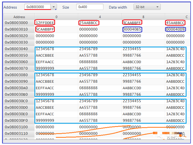
The above screenshot is the content of part of the FLASH space inside the chip after running. The data enclosed by the 5 red boxes is the result of 5 words programming, the data in the blue box is the result of 5 half-page programming, but in the end only 3 half-pages of the programming content are seen, that is Because the content of the next two half pages disappeared after the page erase operation.
The counting frequency of the timer used to count the programming time is 1MHz. Obviously Period1 and Period2 are basically the same. After dividing them by 5, the programming time is 3.3ms. Obviously, half-page programming is more efficient when performing bulk code programming.
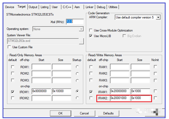
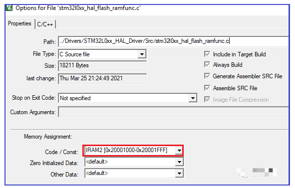
As mentioned earlier, the execution code of half-page programming needs to be put in RAM to run. The code is in the file stm32l0xx_hal_flash_ramfunc.c of the STM32cube library. The implementation of this operation is slightly different for different IDEs. Here is a simple configuration based on ARMMDK, and divide the RAM to use it.
The demonstration of STM32L0 series FLASH programming is introduced here, and I hope to help those in need to save some time and energy.